- HOME
- 產品介紹
- 半導體事業部
- Hamamatsu Photonics
- Image Sensor
- Image Sensors for Near Infrared Region
Image Sensors for Near Infrared Region
![]() +886-2-8772-8910
+886-2-8772-8910
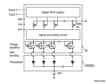
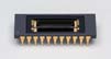
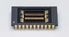
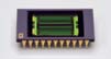
InGaAs image sensors are designed for a wide range of applications in the near infrared region. Built-in CMOS ROIC readout circuit allows easy signal processing. These image sensors use a charge amplifier mode that provides a large output signal by integrating the charge, making them ideal for low -light-level detection.
Equivalent circuit (InGaAs linear image sensor)
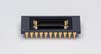
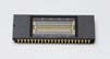
G9201 to G9208 series, etc. |
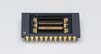
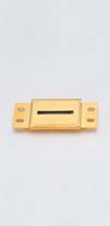
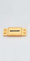
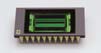
G12230-512WB |
|
 |
 |
|
Type no. |
Cooling |
Pixel |
Pixel pitch |
Number of |
Line rate |
Spectral |
Defective |
Photo |
|---|---|---|---|---|---|---|---|---|
|
G9203-256D |
Non-cooled |
500 |
50 |
256 |
1910 |
0.9 to 1.7 |
0 |
|
|
G9204-512D |
25 |
512 |
960 |
|
||||
|
G11608-256DA |
50 |
256 |
17200 |
0.5 to 1.7 |
1% max. |
|
||
|
G11608-512DA |
25 |
512 |
9150 |
|
||||
|
G9211-256S |
One-stage TE- cooled (Td=-10 °C) |
250 |
50 |
256 |
1910 |
0.9 to 1.67 |
1% max. |
|
|
G9212-512S |
25 |
512 |
960 |
|||||
|
G9213-256S |
500 |
50 |
256 |
1910 |
||||
|
G9214-512S |
25 |
512 |
960 |
|||||
|
G9201-256S |
250 |
50 |
256 |
1910 |
0 |
|||
|
G9202-512S |
25 |
512 |
960 |
|||||
|
G9203-256S |
500 |
50 |
256 |
1910 |
||||
|
G9204-512S |
25 |
512 |
960 |
|||||
|
G9205-256W |
Two-stage TE- cooled (Td=-20 °C) |
250 |
50 |
256 |
1910 |
0.9 to 1.85 |
5% max. |
|
|
G9206-256W |
0.9 to 2.05 |
|||||||
|
G9206-02 |
0.9 to 2.15 |
|||||||
|
G9207-256W |
0.9 to 2.25 |
|||||||
|
G9208-256W |
0.9 to 2.55 |
|||||||
|
G9205-512W |
25 |
512 |
960 |
0.9 to 1.85 |
||||
|
G9206-512W |
0.9 to 2.15 |
|||||||
|
G9208-512W |
0.9 to 2.55 |
These are linear image sensors with high-speed data rate designed for industrial measuring instruments.
|
Type no. |
Cooling |
Pixel |
Pixel pitch |
Number of |
Line rate |
Spectral |
Defective |
Photo |
|---|---|---|---|---|---|---|---|---|
|
G9494-256D |
Non-cooled |
50 |
50 |
256 |
7100 |
0.9 to 1.7 |
1% max. |
|
|
G9494-512D |
25 |
25 |
512 |
3720 |
|
|
Type no. |
Cooling |
Pixel |
Pixel pitch |
Number of |
Line rate |
Spectral |
Defective |
Photo |
|---|---|---|---|---|---|---|---|---|
|
G10768-1024D |
Non-cooled |
100 |
25 |
1024 |
39000 |
0.9 to 1.7 |
1% max. |
|
|
G10768-1024DB |
25 |
|
Type no. |
Cooling |
Pixel |
Pixel pitch |
Number of |
Line rate |
Spectral |
Defective |
Photo |
|---|---|---|---|---|---|---|---|---|
|
G11135-256DD |
Non-cooled |
50 |
50 |
256 |
14000 |
0.95 to 1.7 |
1% max. |
|
|
G11135-512DE |
25 |
25 |
512 |
8150 |
|
|||
|
G11620-128DA |
500 |
50 |
128 |
30800 |
|
|||
|
G11620-256DA |
256 |
17200 |
|
|||||
|
G11620-256DF |
25 |
256 |
17200 |
|
||||
|
G11620-512DA |
512 |
9150 |
|
|||||
|
G11620-256SA |
One-stage TE-cooled (Td=-10 °C) |
500 |
50 |
256 |
17200 |
0.95 to 1.67 |
|
|
|
G11620-512SA |
25 |
512 |
9150 |
|||||
|
G12230-512WB |
Two-stage TE-cooled (Td=-20 °C) |
250 |
25 |
254 + 254 |
9150 |
0.95 to 2.15 |
2% max. |
|


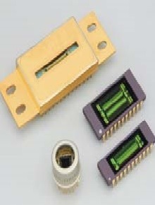
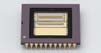
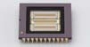
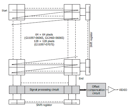
The InGaAs area image sensors have a hybrid structure consisting of a CMOS readout circuit (ROIC: readout integrated circuit) and back-illuminated InGaAs photodiodes.
|
Type no. |
Cooling |
Pixel |
Pixel pitch |
Number of |
Line rate |
Spectral |
Defective |
Photo |
|---|---|---|---|---|---|---|---|---|
|
G11097-0606S |
One-stage TE-cooled (Td=25 °C) |
50 |
50 |
64 × 64 |
1025 |
0.95 to 1.7 |
1% max. |
|
|
G11097-0707S |
128 × 128 |
279 |
|
|||||
|
G12460-0606S |
One-stage TE-cooled (Td=0 °C) |
64 × 64 |
1025 |
1.12 to 1.9 |
|
|||
|
G12242-0707W |
Two-stage TE-cooled (Td=15 °C) |
20 |
20 |
128 × 128 |
258 |
0.95 to 1.7 |
1% max. |
|
|
G13393-0808W |
320 × 256 |
228 |
0.37% max. |
|
||||
|
G13393-0909W |
640 × 512 |
62 |
|
|||||
|
G13441-01 |
Two-stage TE-cooled (Td=-20 °C) |
50 |
50 |
192 × 96 |
867 |
1.3 to 2.15 |
1% max. |
|


檔案下載