- HOME
- 產品介紹
- 半導體事業部
- Hamamatsu Photonics
- Image Sensor
Various types of image sensors covering a wide spectral response range for photometry.
Hamamatsu Photonics develops and manufactures image sensors with high sensitivity and a wide dynamic range that are ideal for high precision measurement such as spectrophotometry, as well as industrial measurement. To help you select the best devices, we offer a wide product lineup that covers a broad spectral range from the near infrared (NIR) at long wavelengths up to 2.6 um through the visible, ultraviolet, vacuum ultraviolet (VUV) on down to the X-ray wavelength region.
Image sensor technology of Hamamatsu
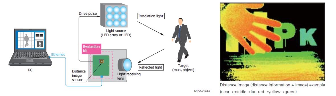
Distance image sensor
This image sensor can detect distance information for the target object using the TOF (time-of-flight) method. A distance measurement system can be configured by combining a pulse-modulated light source and a signal processing section.
Example of distance measurement diagram
Compact thin COB (chip on board) package technology
|
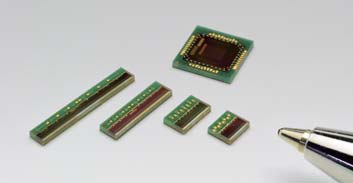
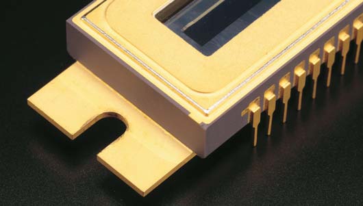
Small mount area can be achieved by mounting the CMOS image sensor chip on a compact thin COB package that is about the same size. In a COB package, the chip is sealed in a resin mold, which provides high reliability and ease of use. CMOS image sensors that employ this technology can be used in a wide range of applications. They contribute to cost reduction, size reduction, and high-volume production of equipment. This technology makes our single 3.3 V power supply operated, low power consumption, high sensitivity CMOS image sensors even more easier to use.
|
 |
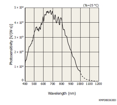
Our unique photosensitive area technology provides high sensitivity in the near infrared region.
|
Spectral response (typical example)
|
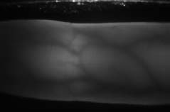
Imaging example of finger veins using near infrared enhanced CMOS area image sensor
|
|
 |
|
|
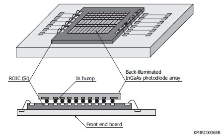
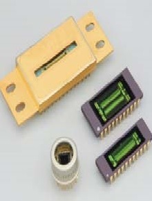
InGaAs image sensors for near infrared region employ a hybrid structure in which the photodiode array used as the photosensitive area and the CMOS signal processing circuit are implemented in separate chips and mounted in three dimensions using bumps. This is used when it is difficult to make the photosensitive area and the signal processing circuit monolithic. Moreover, this construction is advantageous in that the shape of the photosensitive area, spectral response, and the like can easily be modified.
|
Schematic diagram of InGaAs area image sensor using fine-pitch bumps
|
|
 |
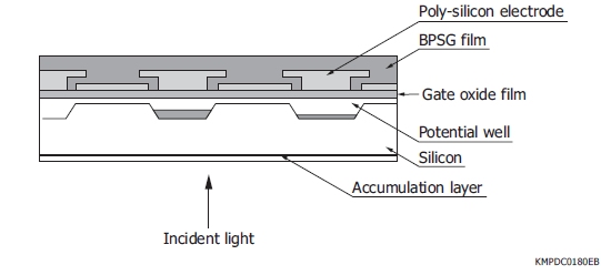
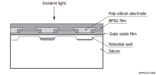
![]() Schematic of CCDs
Schematic of CCDs
|
Back-thinned type
|
Front-illuminated type
|
|
 |
 |
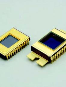
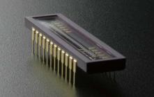
NMOS linear image sensor
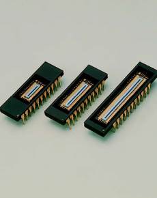
CCD linear image sensor
CMOS linear images sensor
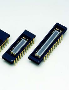
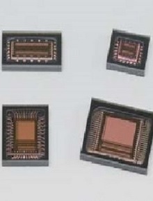
Front-illuminated type CCD area image sensor
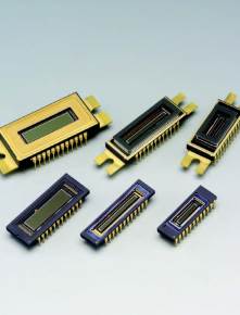
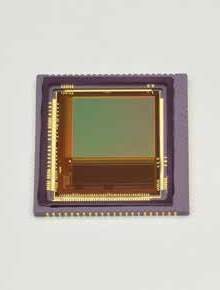
CMOS area image sensor
Back-thinned type CCD area image sensor
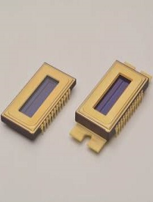
X-ray image sensor
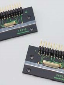
Multichannel detector head
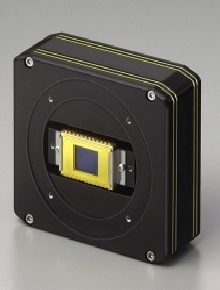
Image Sensors for Near Infrared Region
Distance image sensors
Photodiode Arrays with Amplifier
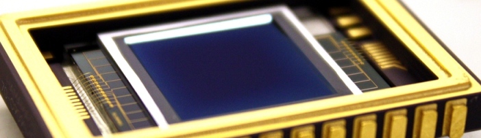
Back-thinned TDI
Back-thinned TDI (time delay integration)-CCDs allow acquiring high S/N images even under low-light conditions during high-speed imaging and the like. TDI operation yields dramatically enhanced sensitivity by integrating the exposure of a moving object. The back-thinned structure ensures high quantum efficiency over a wide spectral range from the ultraviolet to the near infrared region (200 to 1100 nm).
FFT-CCD area image sensor
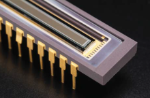
Image Sensor
Back-thinned TDI (time delay integration)-CCDs allow acquiring high S/N images even under low-light conditions during high-speed imaging and the like. TDI operation yields dramatically enhanced sensitivity by integrating the exposure of a moving object. The back-thinned structure ensures high quantum efficiency over a wide spectral range from the ultraviolet to the near infrared region (200 to 1100 nm).
![]() +886-2-8772-8910
+886-2-8772-8910